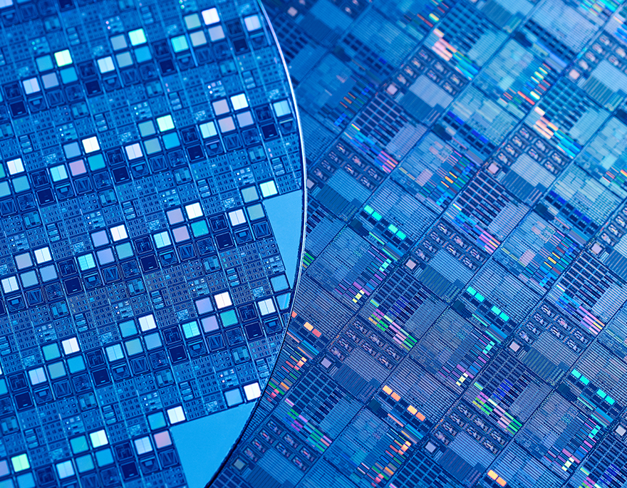
MEMS
Microelectromechanical systems (MEMS) play an important role in industries and sectors that focus on miniaturisation. MEMS are used in aerospace, medicine and industrial automation industries. They feature at least one micro-scale dimension and a wide range of applications, including, among others, pressure sensors, accelerometers, microphones, light sensors and micro motors. The most compact and cost-effective microcircuits are silicon-based (Si), but have some disadvantages, such as high coefficient of friction and low strength. Researchers are therefore investigating new solutions based, for example, on DLC coatings.
DLC coatings
Thin DLC (diamond-like carbon) coatings have a number of applications in microelectromechanical systems (MEMS) due to their unique physical and chemical properties. They are distinguished by their hardness, low coefficient of friction and high thermal conductivity. We provide advanced circuits and automated systems that support research works on the latest technologies. These include PLD (Pulsed Laser Deposition) systems that guarantee full control over parameters such as structure, mechanical properties and water repellency, as well as versatile systems used in the combination of a single or several deposition systems.
Piezoelectrics
Thin-film piezoelectrics have applications in microelectromechanical systems (MEMS), including pressure, vibration and speed sensors. New scientific developments are enabling the development of piezoelectric materials and their various applications in both electronics and medicine. In combination with miniaturization and material technology it is possible to obtain new structures with improved parameters and properties. PREVAC’s wide range of reliable and precise deposition and characterization systems enables research equipment and vacuum techniques to be tailored to individual needs and even the most stringent requirements of scientific projects.
Micro-optical systems
Group III/V semiconductors are used in many fields of science due to their unique physical and chemical properties. Their applications cover a wide range of optoelectronics – from displays to semiconductor devices, which are subject to continuous miniaturization. The development of these technologies is made possible, among other things, by ultra-thin film deposition techniques using molecular beam epitaxy (MBE). For such research work, we offer MBE systems that enable the deposition of thin layers of semiconductors in microelectromechanical systems (MEMS) and nanostructures, under precisely controlled and reproducible conditions. PREVAC systems are distinguished by their versatile design and have the ability to characterize in-situ topography, crystallography, layer thickness and other parameters. All this makes our systems meet the most stringent requirements in semiconductor testing.