Ask about product

Semi-industrial MS systems

Semi-production HV system for fast and repeatable processes of applying thin layers with maximally automated operation support.

Process chamber design allows for a combination of several deposition techniques, among others: DC/RF magnetron sputtering, reactive sputtering, and evaporation using an electron beam. The electronics cabinet with an integrated computer equipped with a large touch screen and user-friendly software will make the coating process of your substrate smooth and easy.

SKU: 327 Category:

Features

  • Automated HV unit for semi-production coating purposes
  • Ideally suited for depositing metal and dielectric thin films
  • Standard size of process chamber: Ø 570 mm
  • Configuration of sources: 2 x 3″ magnetrons and 6-pocket electron beam evaporator (other configurations available)
  • Base pressure range from < 3×10⁻⁷ mbar
  • 2-axes manipulator with stable, long-life heater element to achieve high temperatures up to 300 °C 
  • A wide range of substrate holders size (from 10×10 mm to 6 inches, other on request) and shape
  • Sputter-up and sputter-down arrangement for magnetron sources are available
  • Operated in DC, RF and pulsed-DC modes
  • Ar gas automatic dosing by mass flow control 
  • Possibility for in situ characterization tools, e.g. plasma emission monitor (PEM), ellipsometer, reflectometer, quartz balance or pyrometer temperature measurement system
  • Multiple sources supplied with single power supply and switching networks, or with multiple supplies for co-deposition processing
  • Front door access for fast & easy substrate loading
  • 19“ cabinet with advanced electronic units and dedicated Human-Machine Interface (HMI) device for hardware easy controlling and monitoring process
  • A rigid main frame on wheels allows for easy placement of the system

Description

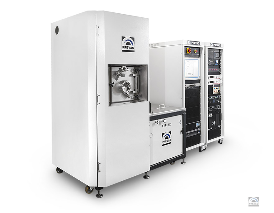
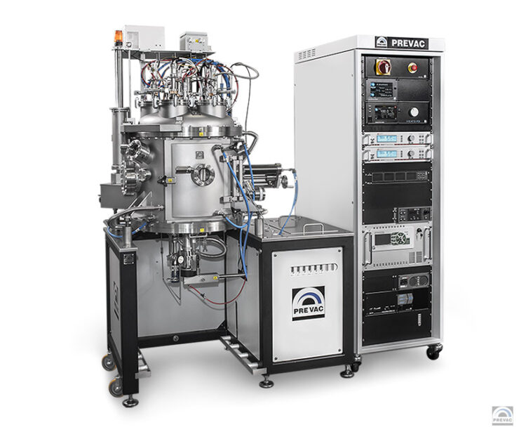
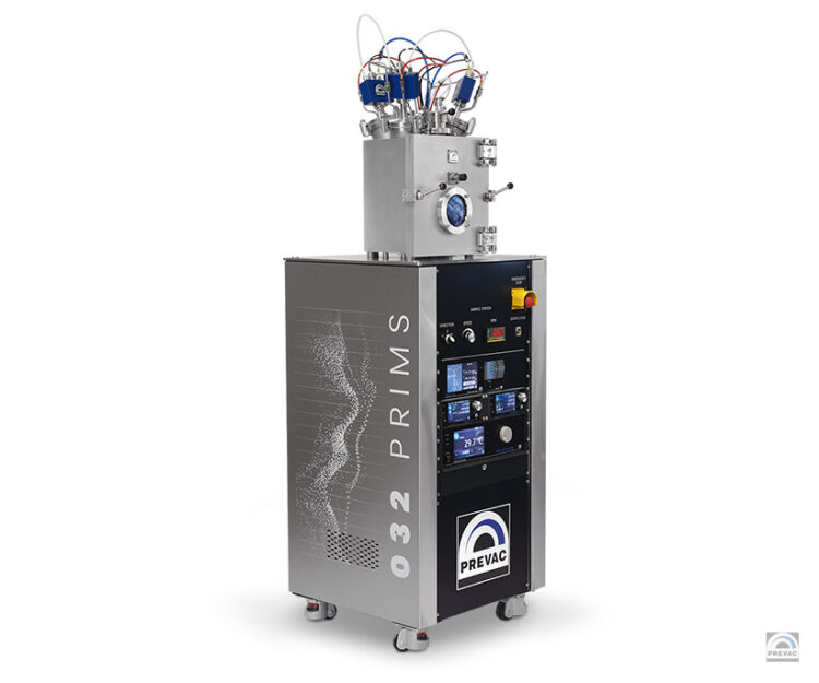
For user convenience, the main chamber is accessible through the front door, so it’s easy to change the magnetrons target, substrate or service/clean the chamber interior. Made from stainless steel, the main chamber is ready for a base pressure range <3*10-7 mbar. In standard, it is equipped with two 3-inch magnetron sources (DC, RF) and a 6-pocket electron beam evaporator. A manipulator with rotation is capable to operate the sample holder up to 6 inches.

The software is mainly aimed to:

  • full control of the deposition system,
  • auto, manual and programmable timer for effective shutter control,
  • graphical system state presentation,
  • process creator and controller,
  • fast, real-time data preview,
  • real-time data acquisition (integration with LIMS data acquisition system).

The system is equipped with advanced, easy-to-use power supplies and electronic devices controlling and supporting the sources and the whole included research equipment.

Options

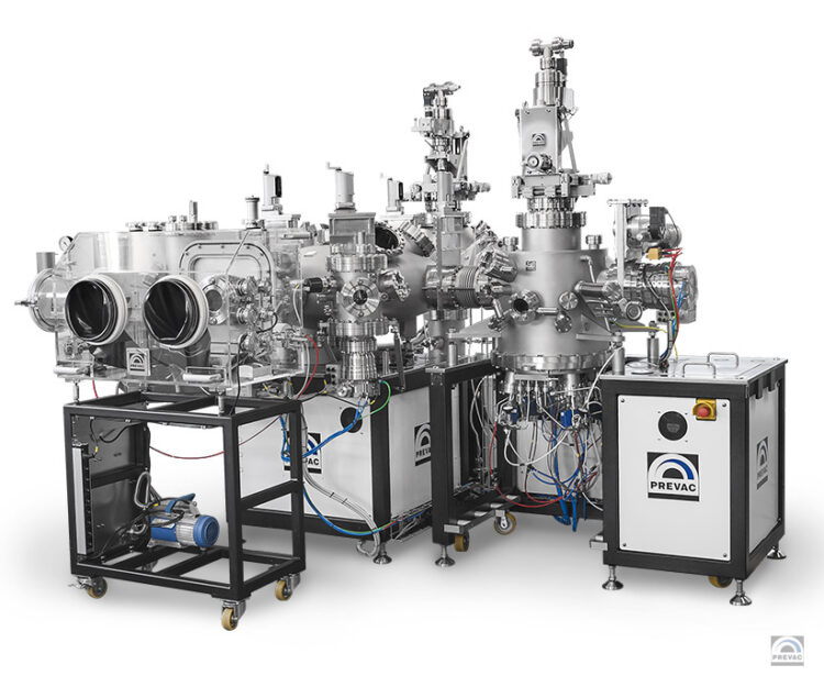
Range of ancillary equipment for streamlining the sputter process is available: 

  • pyrometer – digital pyrometers are used for non-contact, point-shaped temperature measurement in wide range,
  • ellipsometer – analyzes reflected light to determine the thickness and refractive index of dielectrics, semiconductors, and thin metal films. It uses light reflected off the film at a low incident angle,
  • reflectometer – non-invasive tool for fast, real-time measurements of deposition rates, film thickness, layers uniformity, optical constants by spectral reflectance system,
  • plasma emission monitor (PEM) – optical emission spectroscopy technique for real-time plasma monitoring without affecting it,
  • water cooling shroud – as an option the chamber can be equipped with H2O shroud, when there is necessity to decrease components/process temperature,
  • shield protection against cross contamination,
  • motorised shutter (following the substrate) for sputter deposition with thickness gradient,
  • additional gas dosing eg. for the reactive sputtering process,
  • heated viewports for diagnostic,
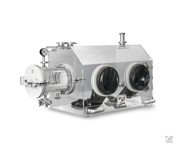
  • glovebox.

Applications

Applications Examples
Single and multilayer conductor films (for microelectronics and semiconductor devices)  Al, Mo, Mo/Au, Ta, Ta/Au 
Barrier layers for semiconductor metallizations  TiN, W-Ti 
Magnetics films  Fe, Co, Ni, Fe-Al-Si, Co-Nb-Zr, Co-Cr, Fe-Ni-Cr, Fe-Si, Co-Ni-Cr, Co-Ni-Si  
Optical coatings – metallic (reflective)  Cr, Al, Ag 
Optical coatings – dielectric  MgO, TiO2, ZrO2 
Photomasks  Cr, Mo, W 
Transparent gas/vapor permeation barriers  Al2O3 
Transparent electrical conductors  InO2, SnO2,In-Sn-O (ITO) 

You may also like…

Ask about product